
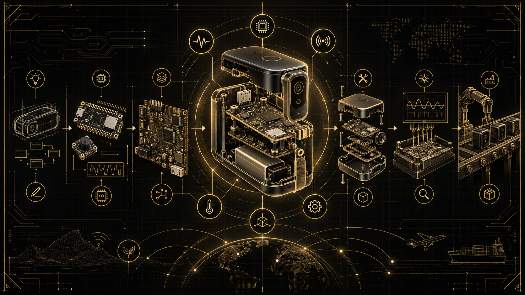
From Idea to Market-Ready Prototype: The Complete Engineering Guide to Developing a Technology Product
A complete zero-to-expert engineering guide to transforming a technology product idea into a functional, validated, manufacturable, and market-ready prototype — covering requirements, feasibility, architecture, electronics, firmware, mechanics, prototyping, verification, cost, compliance, security, DFM, testing, and pr