Some of the hardest work in modern electronics is invisible in the finished product: the routing of a high-speed memory interface between an FPGA and a DDR3 SDRAM. When it is done well, the system simply runs — fast, stable, reliable. When it is done poorly, the board may boot most of the time, fail intermittently under temperature, corrupt data at high utilisation, or refuse to reach its rated speed at all. The difference lies almost entirely in the physical implementation of the interface: the stackup, the impedance, the length matching, the return paths and the power delivery.
This guide comes out of exactly that kind of work — a real FPGA-to-DDR3 interface where high-density BGA fanout, DQ/DQS/address/command routing, length matching, controlled impedance, via strategy, continuous reference planes and crosstalk control all had to come together in a very dense board area. It is written to take you from the fundamentals to genuine mastery of the subject. It is long on purpose: DDR3 layout is a discipline where the details are the design, and every one of them matters. By the end you will understand not just what to do, but why each rule exists.
1. Why DDR3 routing is genuinely hard
DDR3 transfers data on both edges of a clock that can run up to about 1066 MHz, giving data rates from roughly 800 up to 2133 megatransfers per second. At 1600 MT/s a single data bit lasts only about 625 picoseconds, and the usable timing window inside that is a fraction of it. Signals travel across the board at roughly 150–180 ps per inch, so a length mismatch of just a few tenths of an inch between two bits can consume the entire margin. In other words, the copper geometry on your board is part of the timing budget. This is why DDR3 layout cannot be treated as ordinary routing.
Three properties make the interface especially demanding:
- It is source-synchronous. Data is not sampled against a distant system clock; each group of eight data bits travels with its own strobe (DQS), and the receiver clocks the data with that strobe. This is powerful, but it means the relationship between each data bit and its strobe must be preserved in copper.
- Much of it is bidirectional. The data lines drive from the FPGA on writes and from the DRAM on reads, so the topology and termination must work in both directions.
- Margins are tiny and multi-dimensional. Timing, signal integrity, crosstalk, power-supply noise and reference-plane continuity all eat into the same small window, and a failure in any one of them shows up as an unreliable memory.
2. DDR3 fundamentals for the PCB designer
You do not need to be a memory architect to lay out DDR3, but you must understand a handful of electrical facts, because every layout rule flows from them.
Signaling: SSTL-15
DDR3 uses SSTL-15 (Stub Series Terminated Logic at 1.5 V; the low-power variant DDR3L runs at 1.35 V). The I/O supply is VDDQ = 1.5 V, and a receiver decides a logic level by comparing the signal against a reference voltage VREF = VDDQ/2 = 0.75 V. Because the decision threshold sits in the middle of the swing, anything that shifts VREF or adds noise directly steals margin. DDR3 has external reference pins — VREFDQ for the data receivers and VREFCA for the command/address receivers — so the board must supply clean, precise 0.75 V references.
The signal groups
Every DDR3 pin belongs to one of three groups, and each group has its own routing rules. Getting this taxonomy clear in your head is the single most useful thing you can do before routing.
| Group | Signals | Direction / topology |
|---|---|---|
| Data (per byte lane) | DQ[7:0], DQS/DQS# (differential strobe), DM (data mask) | Bidirectional, source-synchronous, point-to-point per device |
| Address / Command / Control | A[n:0], BA[2:0], RAS#, CAS#, WE#, CS#, CKE, ODT, RESET# | Unidirectional (controller → DRAM), fly-by across devices |
| Clock | CK / CK# (differential) | Unidirectional, fly-by, the timing reference for address/command |
The data group is organised into byte lanes: eight DQ bits, one differential DQS strobe and one DM mask per lane. A x16 DRAM has two byte lanes; a 64-bit DIMM has eight. The crucial idea is that each byte lane is its own little source-synchronous bus — the eight DQ bits are captured by their own DQS. That is why matching is done within a lane, to the DQS, rather than across the whole bus.
3. Topology: point-to-point data, fly-by everything else
Topology is the shape of the connection — how a net travels from the driver to one or more receivers. DDR3 deliberately uses two different topologies, one for data and one for address/command/clock, and understanding why is fundamental.
Data lines are point-to-point. Each byte lane connects the FPGA to exactly one DRAM byte, a clean driver-to-receiver link. Point-to-point routing keeps the signal integrity high because there are no branches to create reflections.
Address, command, control and clock use a fly-by topology. Instead of a star that branches to every DRAM (which DDR2 used), DDR3 runs a single trace that passes each device in turn, like a bus tapped in series, with a termination resistor to VTT at the far end. Fly-by dramatically improves signal integrity on these many-load nets by eliminating stubs and reflections — but it creates a deliberate skew: the clock and address arrive at the near device earlier than at the far device.
Fly-by address / command / clock:

  FPGA ──┬──────┬──────┬──────┬────[ Rterm ]── VTT
         │      │      │      │
       DRAM0  DRAM1  DRAM2  DRAM3     (each device taps the same line)


Point-to-point data (one byte lane per device):

  FPGA  DQ[7:0]+DQS  <───────────>  DRAM   (bidirectional, no branches)
That deliberate fly-by skew is corrected not by copper but by the controller, using a calibration step called write leveling (covered later). This is the first appearance of a theme that runs through the whole subject: the PCB gets the timing close, and the FPGA's calibration closes the rest.
4. Termination: VTT, ODT, series resistors and VREF
Every high-speed line must be terminated so that its energy is absorbed at the end instead of reflecting back and corrupting the waveform. DDR3 uses a combination of techniques, and the layout must physically support each one.
- VTT termination for fly-by nets. The address, command, control and clock lines end in resistors (typically around 40–50 Ω) pulled to a VTT rail at VDDQ/2 (0.75 V). VTT must both source and sink current as the lines switch, so it needs a dedicated tracking/termination regulator (for example a TI TPS51200-class part) placed close to the termination resistors, with generous decoupling. Physically, the termination resistors sit at the electrical end of the fly-by chain, past the last DRAM.
- On-Die Termination (ODT) for data. Because the data lines are bidirectional and point-to-point, they use ODT — termination resistors inside the FPGA and the DRAM that switch in and out dynamically during reads and writes. This means the DQ/DQS lines usually need no external termination resistors, which is essential given how many of them there are.
- Series source termination. Small series resistors are sometimes placed at the driver to damp reflections and tune edge rates; whether you need them depends on the controller guidelines and simulation.
Generating VREF. The two reference rails (VREFDQ and VREFCA) must track VDDQ/2 exactly and stay quiet. The classic approach is a precise, well-decoupled resistor divider from VDDQ, or a dedicated reference buffer; the reference is then routed as a quiet, guarded trace to the VREF pins and decoupled right at each pin. Never let VREF pick up switching noise — it is the yardstick every receiver measures against.
5. Stackup and controlled impedance
The stackup is the foundation of everything else. DDR3 routing needs controlled-impedance traces, which is only possible with a well-defined layer stack and a fabricator who builds to your impedance targets.
Typical targets (always confirm against your controller and DRAM vendor guidelines and your fab's capabilities):
- Single-ended signals: around 40–50 Ω (many DDR3 designs use 40 Ω; some use 50 Ω).
- Differential pairs (DQS, CK): around 80–100 Ω differential.
The two non-negotiable rules of the stackup are: every high-speed signal layer must be adjacent to a solid reference plane (preferably ground), and the return current must have an uninterrupted path directly beneath the signal. A DDR3 interface simply cannot be routed reliably on a two-layer board; realistic designs use six, eight or more layers so that data can escape the BGA on inner layers while always referencing a continuous plane.
6. BGA fanout and escape routing
Both the FPGA and the DRAM arrive as ball-grid arrays (BGAs) with dozens to hundreds of balls on a fine pitch. Before any signal can be routed, it must first escape from under the package — and in a dense DDR3 design this fanout is often the hardest and most decisive part of the layout.
The main techniques:
- Dog-bone fanout: a short trace from the pad to an adjacent via that drops the signal to an inner layer. This works for coarser pitches (around 0.8 mm and above) where there is room for a via between balls.
- Via-in-pad: the via is placed directly in the BGA pad (filled and plated over). This is essential for fine-pitch parts where there is no space for a dog-bone, and it also shortens the stub, but it costs more to fabricate.
- Layer planning for escape: the order in which byte lanes escape onto inner layers must be planned so that each group stays together and reaches its destination without crossing plane splits or other groups.
A professional habit is to plan the FPGA pinout with routing in mind. Modern FPGA tools let you assign which bank and which pins carry each byte lane; choosing an assignment that lets each byte lane escape cleanly toward its DRAM — with DQ bits grouped around their DQS — can turn an impossible layout into a straightforward one. Fanout is not a task you do after pin assignment; it should influence the pin assignment itself.
7. Length matching and skew control — the heart of the design
If there is one thing DDR3 layout is famous for, it is length matching. Because the interface is source-synchronous, what matters is not the absolute length of any trace but the relative timing between signals that must arrive together. The rules follow directly from the topology.
| What is matched | To what | Why / typical tightness |
|---|---|---|
| The 8 DQ bits + DM of a byte lane | their own DQS pair | So data and strobe stay aligned; tight — often within a few tens of mils / a few ps |
| Intra-pair skew of DQS and of CK | the two halves of each differential pair | Keeps the differential crossing clean; very tight (a few mils) |
| Address / command / control | the CK clock | So they are sampled correctly on the fly-by bus; matched to a defined window |
| Byte lane to byte lane | each other | Looser — each lane is independent, but usually kept within a broader window |
The exact numbers come from your controller and DRAM vendor's guidelines and your target speed — they are given as length or time tolerances, and faster interfaces demand tighter matching. Two practical points matter more than the specific numbers:
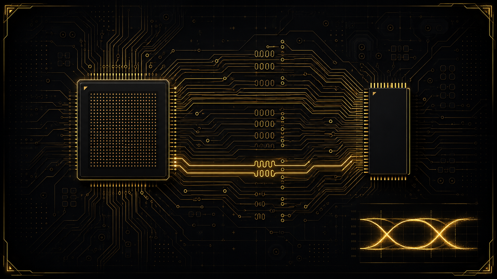
- Match to time, not just to length. A signal on an inner (stripline) layer travels at a different speed than one on an outer (microstrip) layer. Matching physical length across layers can still leave a timing mismatch, so serious tools match on propagation delay and account for the layer.
- Serpentine carefully. To equalise lengths you add meanders (serpentines), but tight serpentines couple to themselves and can add crosstalk; keep enough spacing between the folds and avoid over-tuning.
The freedom you do have: swizzling
Length matching sounds rigid, but DDR3 gives you two powerful degrees of freedom that make dense routing possible:
- DQ bits within a byte lane can be swapped freely. The controller does not care in which order the eight data bits of a lane are wired, as long as the same mapping is used for writes and reads and DQS stays with its lane. This lets you route the eight bits in whatever order is geometrically cleanest.
- Whole byte lanes can be swapped. Which byte lane goes to which DRAM byte is also flexible, because each lane is independent.
This bit- and byte-swizzling is one of the most useful practical tricks in DDR3 layout — it turns a knot of crossing traces into clean, parallel routing. The one rule: DQS must always travel with the byte lane it strobes, and you must reflect any swap in the design so the system knows about it (in DDR3 this is transparent to the controller as long as writes and reads use the same wiring).
Why matching plus training works
Even perfect copper cannot cancel every source of skew — process variation, temperature, voltage and the deliberate fly-by delay all remain. That is why the FPGA memory controller runs a calibration sequence at power-up. Write leveling aligns each byte's DQS to the fly-by clock at that DRAM; read leveling / gate training positions the read strobe correctly; and per-bit deskew fine-tunes individual DQ delays. Length matching gets every signal inside the window that calibration can pull in; calibration then removes the residual. Skip the matching and you hand calibration a problem it cannot solve; do the matching well and calibration has an easy job and the interface is rock-solid over temperature and voltage.
8. Reference planes and return paths
Every signal current flows in a loop: out along the trace and back through the nearest plane, directly underneath the trace, as a return current. At DDR3 speeds this return path is as important as the trace itself, because any interruption in it forces the return current to detour — which adds inductance, distorts the signal, and radiates noise.
The rules that protect the return path:
- Never route a high-speed signal across a split in its reference plane. If the plane beneath the trace changes from ground to a power island or has a gap, the return current cannot follow and the signal integrity collapses. Keep DDR3 signals over continuous planes for their entire length.
- Provide a return path at every layer change. When a signal vias from one layer to another and changes which plane it references, place stitching vias between the two reference planes nearby, so the return current has a low-inductance path to follow the signal. If both layers reference the same ground plane, the ground itself is the return.
- Reference ground where possible. Ground planes make the cleanest, most predictable returns; referencing a switching power plane invites noise.
Return-path discontinuities are one of the most common and most damaging mistakes in high-speed layout precisely because they are invisible on the schematic. The connection is electrically correct; it just performs terribly.
9. Crosstalk and spacing in a dense area
When two traces run close together, a switching aggressor couples energy into a quiet victim — this is crosstalk, and in the tight quarters of a DDR3 fanout it is a constant threat. Crosstalk falls off rapidly with distance, so the primary defence is spacing.
- Follow a spacing rule. A common guideline is to keep trace-to-trace spacing at least three times the trace width (the '3W' rule) for parallel high-speed nets; more where you can afford it, especially for long parallel runs.
- Keep DQS and CK away from aggressors. The strobes and clock are the timing references; couple noise onto them and every bit they capture suffers.
- Minimise parallel run length. Crosstalk accumulates with how far two traces run side by side; break up long parallel sections and route neighbouring groups on different layers where possible.
- Use planes as shields. Signals on adjacent layers that reference a solid plane between them are naturally isolated; broadside-coupled routing without a shield plane invites layer-to-layer crosstalk.
In the densest part of the fanout you cannot always keep ideal spacing, which is exactly why the earlier decisions — pin planning, byte-lane grouping, swizzling — matter so much: they reduce how many signals must crowd together in the first place.
10. Vias, stubs and back-drilling
Every via is a small impedance discontinuity and, on thick boards, a source of stub — the unused portion of the barrel below where the signal actually leaves. A stub acts like a little resonant antenna that degrades the signal at high frequencies. The mitigations:
- Minimise the number of vias on each high-speed net; every transition costs signal integrity and adds a return-path concern.
- Keep transitions symmetric within a matched group so the vias contribute equally to each net.
- Back-drill (or use blind/buried vias) on thick boards or very high speeds to remove the stub. Back-drilling mechanically removes the unused via barrel after plating. For DDR3 speeds this is often unnecessary, but the technique becomes essential as you move to DDR4 and beyond.
- Add ground stitching vias next to signal-layer transitions so the return current follows cleanly.
11. Power delivery and decoupling (PDN)
A DDR3 interface can switch dozens of lines simultaneously, each demanding a burst of current from VDDQ in a fraction of a nanosecond. If the power-distribution network (PDN) cannot supply that current with low impedance across a wide frequency range, the supply sags, ground bounces, and every signal referenced to those rails is corrupted. Power integrity and signal integrity are the same problem seen from two sides.
The essentials of a good DDR3 PDN:
- A low-impedance VDDQ. Use a solid VDDQ plane (or wide pour) with plenty of copper, feeding both the FPGA I/O bank and the DRAM.
- Decoupling from bulk to high frequency. Bulk capacitors handle low-frequency demand; many small high-frequency capacitors placed as close as possible to the BGA power balls handle the fast transients. Placement matters more than value — a capacitor far from the ball is nearly useless at these speeds.
- Dedicated care for VTT and VREF. The VTT rail needs its own regulator and local decoupling because it actively sources and sinks termination current; VREF needs quiet, filtered decoupling right at each pin.
- Plane capacitance. Closely spaced power and ground planes form a natural high-frequency capacitor that helps at the frequencies discrete capacitors cannot reach.
12. The timing budget — where the picoseconds go
Everything above ultimately serves one goal: keeping the data valid at the receiver long enough, and stably enough, to be sampled correctly. The receiver needs the data to be stable for a setup time before the strobe and a hold time after it. The bit period is short, and it is spent by many contributors:
- the driver's clock-to-output delay,
- the flight time along the trace,
- skew between a bit and its strobe (this is what length matching controls),
- inter-symbol interference and reflections (signal integrity),
- crosstalk-induced timing push-out,
- clock and supply jitter,
- and VREF/threshold uncertainty.
Add these up and what remains is your margin. The point of good layout is to keep each term small so the sum leaves a comfortable window — and calibration then centres the sampling point inside it. This is why an experienced designer thinks in picoseconds and millivolts, not just in nets and connections: a length mismatch, a discontinuous return path and a noisy VREF are not separate cosmetic issues, they are three withdrawals from the same tiny timing account.
13. Signal-integrity simulation and verification
Because the margins are so small and invisible, serious DDR3 design is verified with simulation rather than hope. The key tools and steps:
- IBIS / IBIS-AMI models. The FPGA and DRAM vendors supply behavioural models of their I/O buffers (IBIS). These let you simulate the real driver and receiver behaviour without exposing the transistor-level design.
- Pre-layout topology exploration. Before routing, you simulate candidate topologies, termination values and stackups to choose an approach that will work — cheaper than discovering a problem after fabrication.
- Post-layout signal integrity. After routing, the actual geometry is extracted and simulated to check waveforms at the receiver against the DDR3 mask.
- Eye diagrams. The classic verification: overlay many bit periods to form an 'eye', and confirm it is open enough — wide (timing margin) and tall (voltage margin) — with the DDR3 compliance mask fitting inside.
- Timing analysis. Combine flight times, skew and setup/hold to confirm the budget closes across process, voltage and temperature corners.
Common tools for this work include Cadence Sigrity, Siemens HyperLynx, Keysight ADS and the vendors' own reference flows. The exact tool matters less than the discipline: measure, don't assume.
14. The FPGA side: controller, PHY and calibration
The board is only half of the interface; the other half lives inside the FPGA. Modern FPGAs provide a memory controller and PHY — generated by the vendor's tooling (for example AMD/Xilinx's memory interface generator, or Intel's external-memory interface) — that turns the raw DDR3 protocol and the delicate physical timing into a simple user interface. This block:
- drives the SSTL-15 I/O with the correct drive strength and ODT,
- runs the power-up calibration (write leveling, read leveling, per-bit deskew, DQS gating) that compensates for the residual skew your layout left,
- and provides the timing constraints your PCB must meet.
This is why pin planning and layout are not independent of the FPGA design: the tool tells you the length-matching tolerances and byte-lane groupings, and your job is to give it a board it can calibrate. When the layout respects the controller's guidelines, calibration succeeds quietly at every power-up; when it does not, calibration fails or the interface is marginal.
15. A practical layout workflow
Bringing it together, a professional DDR3 layout tends to follow this order:
- Read the guidelines. Start from the DRAM datasheet and the FPGA controller's layout and constraint guide. They define impedance, matching tolerances, topology and termination.
- Plan the pinout and byte lanes. Assign FPGA banks and pins so each byte lane can escape cleanly toward its DRAM, DQ grouped around DQS. Fanout drives pin assignment, not the other way around.
- Define the stackup with your fab. Fix layer count, dielectrics and the impedance targets (single-ended and differential), ensuring every signal layer references a solid plane.
- Fan out the BGAs. Choose dog-bone or via-in-pad per pitch, and escape each group to its routing layer.
- Route data lanes point-to-point, matched within each lane to its DQS, using swizzling to keep the routing clean.
- Route address/command/clock fly-by, matched to CK, ending in VTT termination past the last device.
- Place power and decoupling, with high-frequency capacitors tight to the BGA power balls, and dedicated VTT and VREF networks.
- Tune lengths on propagation delay, keeping serpentines well spaced.
- Simulate and verify with IBIS models, eye diagrams and timing analysis; iterate.
- Review against a checklist before release.
16. Common mistakes and a pre-tapeout checklist
The mistakes that most often ruin a DDR3 board:
- Routing high-speed signals across a plane split or over a gap, breaking the return path.
- Matching physical length across layers instead of matching propagation delay.
- Forgetting stitching vias at layer transitions.
- A noisy or imprecise VREF, or a VTT rail that cannot sink current.
- Too little high-frequency decoupling, or capacitors placed too far from the BGA.
- Excessive via stubs on a thick board at high speed.
- Ignoring the controller's guidelines and hoping calibration will fix everything.
- Over-tight serpentines that add their own crosstalk.
A short pre-release checklist:
- Every DDR3 signal references a continuous plane along its entire length.
- Stitching vias exist at every high-speed layer transition.
- DQ/DM matched to their DQS; DQS and CK intra-pair skew tight; address/command matched to CK — all on propagation delay.
- Impedance targets confirmed with the fabricator.
- VTT termination present past the last device, with its regulator and decoupling.
- VREF precise, filtered and quiet at every pin.
- High-frequency decoupling tight to the BGA power balls.
- Post-layout SI and timing simulated; eyes open with margin.
- Layout matches the controller's constraint file exactly.
Conclusion
Routing a DDR3 interface to an FPGA is one of the clearest demonstrations that in high-speed design, the layout is the engineering. The schematic connection is trivial; the reliability is created — or destroyed — in the physical implementation: the stackup and impedance, the BGA fanout, the length and skew matching, the continuous reference planes and return paths, the crosstalk control, the termination and the power delivery, all verified in simulation and completed by the controller's calibration. Get these right and the memory simply works, at full speed, across temperature and voltage, for the life of the product.
This kind of dense, high-speed hardware — where careful PCB layout and disciplined high-speed routing make the difference between a board that boots and a board that ships — is exactly the work I do. If you are building FPGA-based hardware with DDR3 (or faster) memory, high-density BGA fanout, or any demanding high-speed interface and want it engineered to be reliable from the first prototype, get in touch — I would be glad to help.